Not long ago I built a DIY Cocoquantus Delay. I received a second PC board from Josh Rodriquez, and he reminded me to use it for tracing the delay circuit and recovering a schematic diagram, and in the process learning how the delay works. Now that I’ve done that and grokked the design, here I’m sharing what I learned.
There is a special kind of joy in figuring out how something works. For a circuit you first need a schematic diagram and then gather the datasheets for all the chips. I traced the circuit and created a schematic diagram. I’ve redrawn it in three sections that I’ll describe in turn.
Now here’s the information given by Peter Blasser himself about the digital part of this delay. His schematic drawing of the analog part has enough detail that it can be understood. But not so his digital drawing.
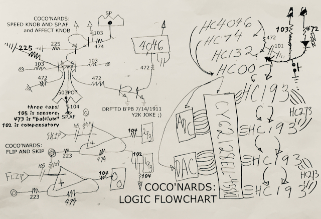
Consider Peter’s drawing, above. In the upper left corner is the analog circuit for controlling the speed of the oscillator, HC4046. We’ll skip that part. The lower left shows the interfaces for the Skip and Flip inputs. The rest of the drawing indicates the logic chips, the ADC (analog to digital converter chip), the DAC (digital to analog converter chip), the memory chip (CY62128), the address counter chips (4 HC193) and the two HC273 chips that implement the Skip function. He also shows the Freeze switch that halts writing new data into the memory.
Control Logic
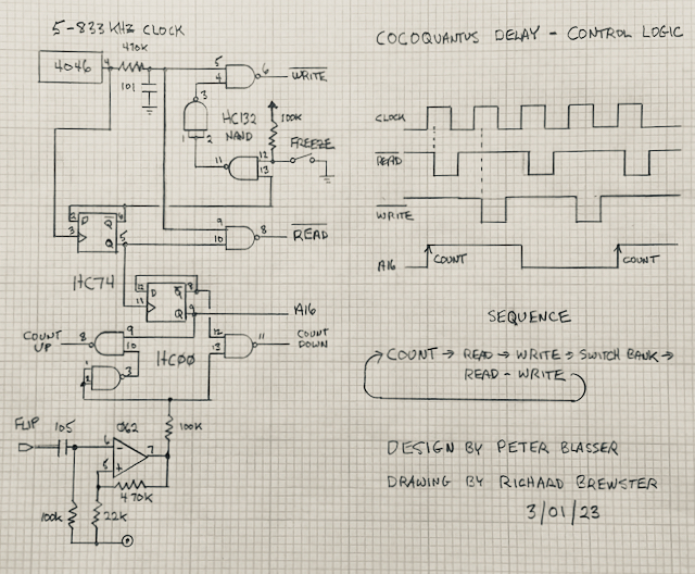
The function of the control logic is to derive control signals from the clock square wave generated by the voltage controlled digital oscillator, the HC4046. The Flip control is integrated here, as well as the Freeze function. The control signal are as follows.
- READ (active low) – Read a value from the memory for output to the DAC.
- WRITE (active low) – Read a value from the ADC into memory
- Count Up – Move the memory position forward
- Count Down – Move the memory position backward
- A16 – Switch memory banks
An input to the Flip jack or touch pad momentarily switches from counting forwards to counting backwards, resulting in both reading and writing in the reverse direction.
Closing the Freeze toggle switch simply stops writes from happening.
The Sequence of Operations
A count happens (either forward or backward) on the rising edge of a clock pulse. A new count occurs every four clock pulses. Midway through the count cycle, A16 switches the bank. Very shortly after the count, because a delay is introduced by an RC network, there’s a Read pulse. Next comes a Write pulse. Thus a memory location is read for output and then overwritten by the current input value. Then the memory bank is switched and another Read-then-Write occurs. A short time later the sequence is repeated. The sequence repeats indefinitely.
The Two Memory “banks”
The memory chip holds 128K bytes. This design writes and reads in bytes (8 bits). That’s why it’s called an 8-bit delay. That sets the resolution to a high of 256 values for the analog conversions. The memory can hold 128K bytes, but our addressing circuit — described in detail later — has 16-bits, A0-A15, and can address 64K of memory. The A16 signal controls the most significant address bit to the memory, A16, which divides the memory into two 64K segments, or banks. As far as the delay goes, it only cares which memory address is next to read and write. It does not care about the where the next memory location is. And, as we’ll see, this design does not step through the address space by incrementing the address value.
A-to-D and D-to-A
Each of these operations is handled by a special chip.

Josh sent me the below image with two clarifications in BLUE. The Coco output, i.e. DELAY OUT, comes from the Wet/Dry mixer, which also goes to the ADC input.
I had labelled the DAC output DELAY OUT. It goes into the Wet/Dry mixer (Josh’s label OTA) as the Wet signal. So you can see how the Wet gets mixed back into the delay input. In this design there’s always an echo, because the Wet has to be mixed with the Dry to get any Wet signal on the output.

Tri-State Data Bus
The eight bit data bus (D0-D7) is shared by the ADC, the DAC, and the memory chip. Three state logic simply means that the data lines can become high impedance (neither 1 nor 0), under control, so that only one of the chips is allowed to put data on the bus at any given time.
Reading a byte from memory and converting to analog for output
From the TLC7524 data sheet:
When CS and WR are both low, analog output on these devices responds to the data activity on the DB0−DB7 data bus inputs. In this mode, the input latches are transparent and input data directly affects the analog output. When either the CS signal or WR signal goes high, the data on the DB0−DB7 inputs are latched until the CS and WR signals go low again.
Interpretation:
CS is tied to ground in this design, so we can ignore it. When our READ signal, controlling WR here, goes low, it does two things. It enables the memory chip to place the data at the current address onto the data bus (see below). At the same time it tells the D-to-A chip to look at the data bus. When WR goes high again the converted value is held at the analog output. Note that writing from the perspective of the DAC chip means putting something onto its output. For this we have to read from memory.
Reading an analog value from the input and writing the converted digital value into memory
We’re using the TLC0820 ADC chip in read/write mode (pin 7 tied high).
Notice that both the Read and Write signals from our control section are used, and that they go to the oppositely named pins on the chip! From the data sheet:
The conversion is started on the falling edge of the WR input signal. The result of the conversion is strobed into the output latch after the internal count-down delay time, td(int), provided that the RD input does not go low prior to this time.
The 3-state data outputs D0 through D7 are activated when RD goes low. As a result, the data transferred to the output latch is latched after the falling edge of RD.
What we’re doing here is starting an A-to-D conversion at the beginning of our READ command, a short time later our WRITE command enables the converted value onto the data bus, where it can be read by the memory chip and stored.
Address Control and Skip Function

A memory chip is pretty simple but has a lot of wires. Eight I/O data lines connect to the shared Data Bus. Seventeen address bits select the memory location to write or read. From the data sheet:
To write to the device, take Chip Enable (CE1 LOW and CE2 HIGH) and Write Enable (WE) inputs LOW. Data on the eight I/O pins (I/O0 through I/O7) is then written into the location specified on the address pins (A0 through A16).
To read from the device, take Chip Enable (CE1 LOW and CE2 HIGH) and Output Enable (OE) LOW while forcing Write Enable (WE) HIGH. Under these conditions, the contents of the memory location specified by the address pins appear on the I/O pins.
Since CE1 and CE2 are always enabled, all we have to be concerned with is our WRITE and READ control signals. Very straightforward.
Counting Up and Counting Down
A sixteen-bit counter is formed from four cascaded HC193 Presettable Up/Down Counter chips. From the HC193 data sheet:
Cascading is effected by connecting the carry and borrow outputs of a less significant counter to the Clock-Up and Clock-Down inputs, respectively, of the next most significant counter.
In the schematic above, the four chips represent the least to the most signification counter, going top to bottom. The bottom chip gets its Count Up and Count Down commands from our control logic.
Using the Preset capability to implement the Skip function
Peter B went to great lengths to make a Skip function. Here’s how it works. The Skip input interface op amp generates a positive going pulse that last for a small period of time. The HC273 chips are eight independent data latches, and their inputs are set by the current output of the counters. On that Skip pulse, the current address values are saved and held at the outputs of the HC273s. Then, when the Skip pulse falls, a Preload signal is sent to all four of the HC193 counters. In the mean time the counters have continued counting. But at when the Skip pulse falls, a Preload signal to the counters causes the saved address to be reloaded, resulting in a skip forward or backward depending on the direction of the count. Counting continues from that address.
Non-incremental addressing
If you look closely at the address line connections to the counters, you can notice that there is an arbitrary correspondence between the significance of the address bits and how they’re driven by the counter outputs Q0-Q3. So the sequence of addresses being used is not going incrementally. The next address can be many locations away from the current one. Yet it doesn’t matter. All that matters is that the same sequence of address locations is generated repeatedly. And, as we’ve seen, indeed each successive location is actually in the opposite bank!
The Yellow Jack
In the lower left of the drawing, below the memory chip, you see twelve resistors glomed together. What Peter did was to combine twelve of the address lines (outputs from the counter chips) into a seemingly random signal you can patch from. It’s that simple.


Very interesting circuit and analysis. Is it possible to have the address control schematic in better resolution? Cant make out lots of the values, thank you
Thanks, Roger. Try right click and save image. You get a .webp file that you may be able to read better.
Added a clarification on the ADC/DAC circuit drawing that Josh Rodriquez sent me today.
Hello Richard !
Do you think it is possible to increase the speed of the oscillator (hc4046) to have shorter delay times ? By changing a cap value or something ?
I know it’s possible to acheive the max speed with ground connected in the spaf but i want to make it way much faster…
Thank you !!
Hi Robin,
There is a 1000pf polystyrene capacitor between pins 6 & 7 on the HC4046. If this was smaller, the minimum and maximum frequencies would increase, making the delay times shorter.
There is a fixed delay after the address (count) is updated, before a read or write is activated. If the clock ran too fast, this fixed delay could introduce problems.
Are you planning to experiment with the value?
Is the reason for the non-incremental address sequencing the effect it has on the yellow jack output? If no, is there any effect the non-incremental address sequencing has?
Hi Todd,
No, the reason for the non-incremental addressing is just to simplify the addressing. It has no effect on the yellow jack output because A16, the bit that switches the memory bank, is not included in the mixture of bits making up the yellow jack out.
Hello Richard, sorry i forgot to answer !
Yes i do plan to mess with this capacitor value to change the delay time, but i don’t see where the fixed delay is ? Maybe i could add a switch somewere wich change the value of the two delays…
Hi Robin,
At pin 4 of the 4046 there is an RC network, a 470K resistor followed by a 100pf cap. This small delay allows the address lines to the memory and to the D/A and A/D chips to settle before a read or write is done. You could try a 470pf cap at pins 6&7 to double the maximum clock speed. I’d try that first. If things go wonky, try replacing that 470K with a 390K or 330K. But if you go too low with this resistor, it might also mess things up. Experiment!
Youpi ! Thank you very much Richard ! I’ll try as soon as i can !